

Introduction
Power divider (PD) is one of the most important passive circuits and is widely used in microwave circuits [Reference Song, Zhang, Hu and Fan1–Reference Liu and Xiao18]. Since the PD has been proposed, great interest has been aroused in developing various kinds of power-dividing/combining circuits, such as waveguide PDs [Reference Song, Zhang, Hu and Fan1–Reference Oh, Lee, Kim and Min3], planar PDs [Reference Song and Xue4–Reference Chen, Huang, Shen and Wu13], and substrate-integrated waveguide (SIW) PDs [Reference Song, Fan and Zhang14–Reference Liu and Xiao18]. SIW techniques are attractive for the design of microwave and millimeter-wave components, due to their high Q factor, low cost, and high integration capability. The half-mode SIW (HMSIW) has been developed in recent years [Reference Jin and Wen19–Reference Chen, Song, Hu and Fan21]. Compared with the SIW, HMSIW is a newly proposed planar structure that keeps the advantages of SIW but the size is nearly half reduced. In [Reference Zou, Tong and Yu22], a Y-junction four-way PD is proposed by integrating the SIW PD and the HMSIM PD.
In this paper, a modified four-way Y-junction PD/combiner that is based on the traditional Y-junction structure is proposed. The proposed divider/combiner is a five-port structure and is capable of producing equal power ratios. The simulated and measured results show that the insertion loss is <1.2 dB for each of the four output ports from 4.5 to 7.0 GHz. The proposed divider/combiner exhibits better than 17 dB return loss with more than 13 dB isolation between adjacent ports in the same frequency range. The theory and design of the proposed PD/combiner are given. The proposed four-way PD is fabricated and measured. The measured results agree with the simulated ones closely.
Analysis of PD/combiner circuit
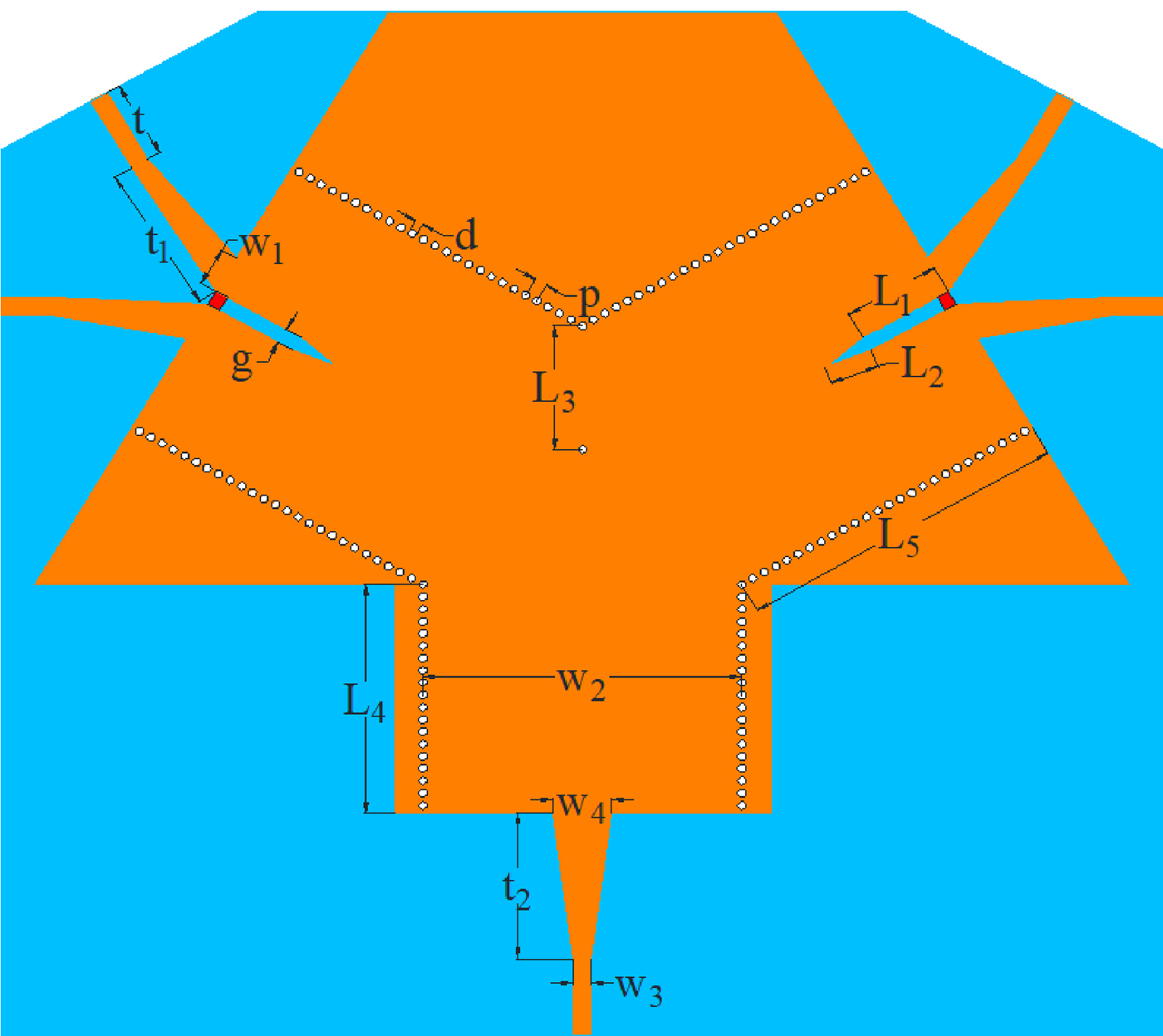
The topology of the modified Y-junction PD/combiner circuit is shown in Fig. 1. The circuit consists of three parts: a Y-junction structure based on SIW and two identical two-way HMSIW PDs. The signal through which the Y-junction structure is divided into two paths and then four output ports is achieved by HMSIW dividers. To improve the isolation between the four output ports, the isolation resistors are set between the two adjacent HMSIW. In addition, only a single substrate is used in the PD/combiner circuit; on the one hand, it is easy to install the isolation resistor, and it can improve the reliability of the circuit.
Topology of modified four-way Y-junction SIW power divider/combiner circuit.
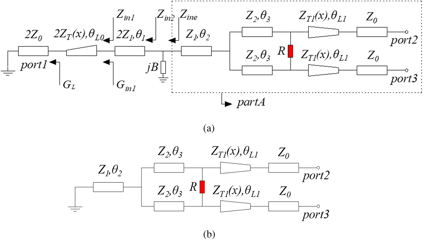
As can be seen, the modified four-way Y-junction PD/combiner is symmetrical, so the even- and odd-mode equivalent circuit analysis can be used. The equivalent circuit of the circuit is shown in Fig. 2. Under the even-mode excitation, a bisection of the PD is shown in Fig. 2(a). Z 0 and Z 1 are the characteristic impedance of microstrip line and SIW. The characteristic impedance of the taper-shaped transition at x can be derived as [Reference Deslandes23]:
 $$Z_{T(x)} \displaystyle{{120\pi} \over {\sqrt {\varepsilon _e} [(w_1 (x)/d) + 1.393 + 0.677\ln ((w_1 (x)/d) + 1.444)]}},$$
where
 $$w_1 (x) = \displaystyle{{x(w_4 - w_3 ) + w_3 t_2} \over {t_2}}, $$
d is the height of the substrate; ε e is the relative permittivity; t 2 is the length of the taper; w 3 and w 4 are the widths of the taper, as shown in Fig. 1. The quarter wavelength taper is sufficient to obtain a good return loss. In any case, taper lengths must be chosen as a multiple of a quarter of a wavelength in order to minimize the return loss. The transmission parameters of a linear tapered TEM transmission line are already known analytically [Reference Lu24] and the widths w 3 and w 4 can be achieved. These equations are used to verify the return loss of the taper over the full bandwidth. According to the end of the taper, the reflection coefficient and the input impedance can be derived as:
 $$\Gamma _{{\rm in}1} = \displaystyle{1 \over 2}\int_0^{t_2} {e^{ - j2\beta x}} \displaystyle{{d[\ln 2Z_T (x)]} \over {dx}}dx + \Gamma _L, $$
 $$Z_{in1} = \displaystyle{{(1 + \Gamma _{in1} )2Z_1} \over {(1 - \Gamma _{in1} )}}.$$
Equivalent circuit model of broadband-modified four-way Y-junction power divider/combiner circuit: (a) even-mode equivalent circuit; (b) odd-mode equivalent circuit.

Thus, the input impedance of the Y-junction Z in2 and the input impedance Z ine can be, respectively, derived as:
 $$Z_{in\,2} = 2Z_1 \displaystyle{{Z_{in1} + 2jZ_1 \tan \theta _1} \over {2Z_1 + jZ_{in\,1} \tan \theta _1}}, $$
 $$Z_{ine} = \displaystyle{{Z_{in\,2}} \over {1 + jBZ_{in\,2}}}. $$
When part A is matched, the total input impedance of the part A circuit is equal to Z 1. The good impedance match can be achieved when:
 $$B = \displaystyle{1 \over {\,jZ_1}} - \displaystyle{{2Z_1 + jZ_{in1} \tan \theta _1} \over {2jZ_1 (Z_{in1} + 2jZ_1 \tan \theta _1 )}}.$$
When part A is matched, the total input impedance of the part A circuit is equal to Z 1. The good impedance match can be achieved when:
 $$Z_{ine} = Z_1. $$
A centrally located via acts as an inductive matching post to nullify the effect of the Y-junction capacitance and therefore promoting lower return loss at the input. The parameter “w 2” determines the propagation constant of the fundamental mode, the diameter of via-holes “d”, and the pitch length of via-holes “p” are set to minimize the radiation loss and the return loss. The “d” and “p” can be achieved according to [Reference Deslandes and Wu25] and the dielectric constant in the frequency normalization allows an almost direct design of SIW junctions using any substrate by determining w 2. The results are valid in the following range [Reference Germain, Deslandes and Wu26]:
 $$0.65 \lt w_2 \sqrt {\varepsilon _r} /\lambda \lt 0.92.$$
Furthermore, it can be found from Fig. 2(a) that part A of the even-mode equivalent circuit can be further analyzed by even and odd modes. The even- and odd-mode equivalent circuits of part A are shown in Fig. 3. As we can see from Fig. 3(a), in the even-mode equivalent circuit, no current flows through the isolation resistor. Thus, the input impedance and reflection coefficient, which are seen from the end of the HMSIW, can be derived as:
 $$Z_{in\,3} = Z_2 \displaystyle{{2Z_1 + jZ_2 \tan \theta _3} \over {Z_2 + 2jZ_1 \tan \theta _3}}, $$
 $$\Gamma _{in\,3} = \displaystyle{{Z_{in\,3} - Z_{T1} (0)} \over {Z_{in\,3} + Z_{T1} (0)}}.$$
Equivalent circuit model of part A: (a) even-mode equivalent circuit of part A; (b) odd-mode equivalent circuit of part A.

The characteristic impedance of the taper-shaped transition at x in the odd-mode equivalent circuit can be derived as [Reference Deslandes23]:
 $${\rm Z}_{T1} (x) = \displaystyle{{120\pi} \over {\sqrt {\varepsilon _e} [(w_2 (x)/d)\! +\! 1.393 + 0.667\ln ((w_2 (x)/d)\! +\! 1.444)]}},$$
where
 $$w_2 (x) = \displaystyle{{t_1 w_1 - (w_1 - w_3 )x} \over {t_1}}, $$
t 1 is the length of the output taper, and w 1 and w 3 are the widths of the taper, as shown in Fig. 1. Seen from the end of the taper, the reflection coefficient and the input impedance can be derived as:
 $$\Gamma _{{\rm in}} = \displaystyle{1 \over 2}\int_0^{t_1} {e^{ - j2\beta x}} \displaystyle{{d[\ln Z_{T1} (x)]} \over {dx}}dx + \Gamma _{{\rm in}3}, $$
 $$Z_{in} = \displaystyle{{(1 + \Gamma _{in} )Z_0} \over {(1 - \Gamma _{in} )}}.$$
The reflection coefficient at the port 2 can be derived as:
 $$\Gamma _0 = \displaystyle{{Z_{in} - Z_0} \over {Z_{in} + Z_0}} = \Gamma _{in}. $$
Therefore, the reflection coefficient of the port 2 can be determined by the above equations, when the port 2 reflection coefficient Γ0 is given. The parameters of microstrip transition can be obtained [Reference Lu24]. As shown in Fig. 3(b), in order to achieve the impedance match, the circuit must satisfy:
 $$\displaystyle{{Z_{in\,2} (R/2)} \over {Z_{in\,2} + R/2}} = Z_{T1} (0),$$
where
 $$Z_{in\,2} = jZ_2 \tan \theta _3. $$
Thus, the isolation resistor must satisfy:
 $$R = \displaystyle{{2Z_{in\,2} Z_{T1} (0)} \over {Z_{in\,2} - Z_{T1} (0)}},$$
when 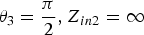 $\theta _3 = \displaystyle{\pi \over 2},Z_{in2} = \infty $. By equation (12.a), resistor can be expressed as:
 $$R = 2Z_{T1} (0).$$
The value of isolation resistor can be determined by equation (12.b). After the initial width of the taper w 1 1 is determined. The Z T1(0) and the value of isolation resistor can be determined. The slot can be determined according to [Reference Eom, Byun and Lee27].
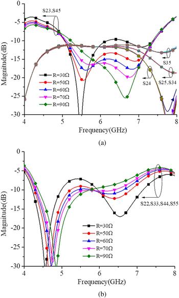
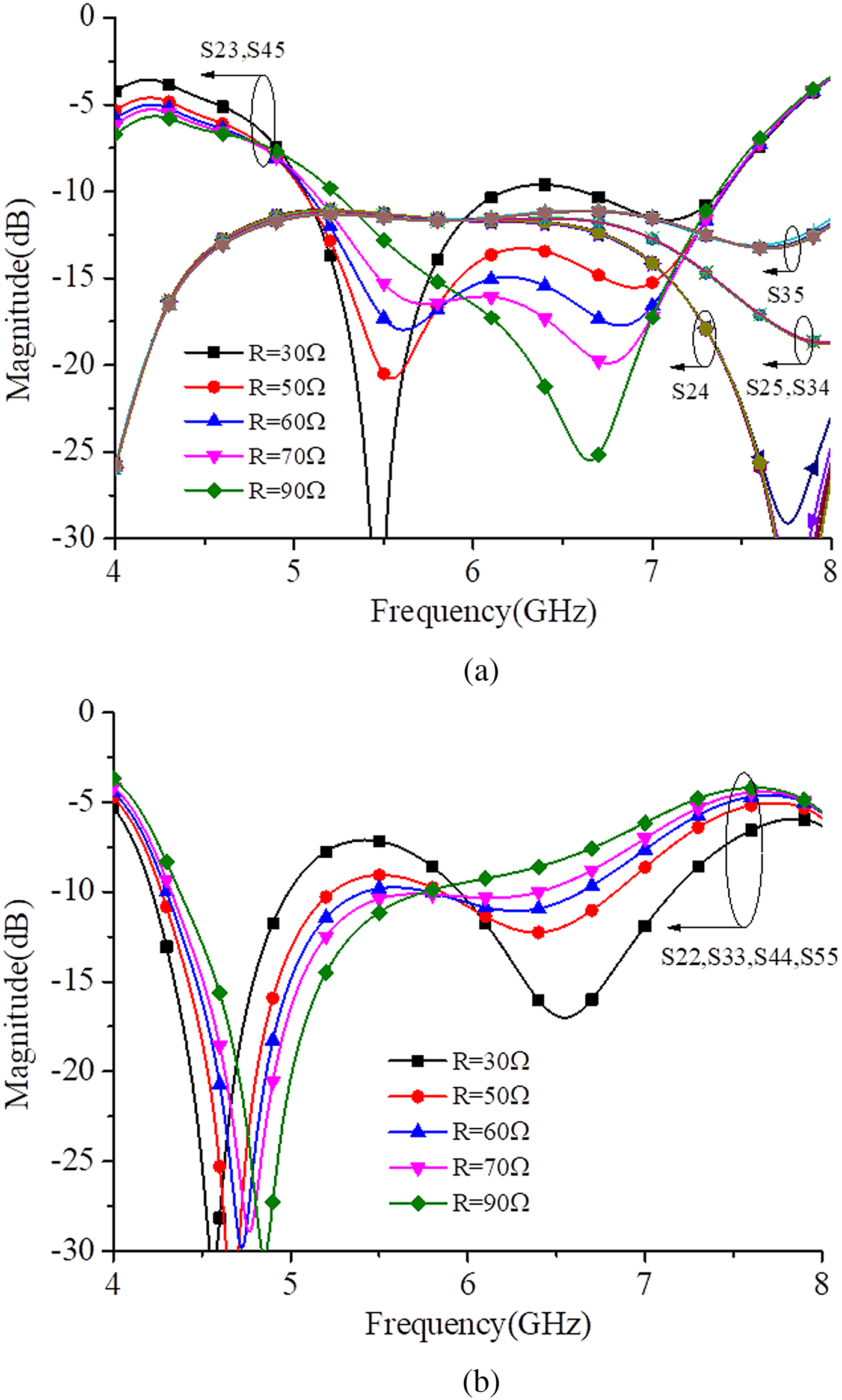
The correctness of above deduction can be verified by the simulation results of the circuit. The relationship between resistor and isolation or return loss when w 1 = 2.5 mm is shown in Fig. 4, when the value of isolation resistor is about 50–60 Ω, the isolation and the VSWR bandwidth are better. When w 1 = 2.5 mm, the Z T1 (0) ≈ 28.9 Ω and R = 57.8 Ω. The simulation and measurement results show good agreement. The final value is R = 51 Ω.
Effect of isolation resistor on circuit isolation and output VSWR: (a) effect on isolation; (b) effect on output VSWR.
Summary of the total design procedure
(a) The width of the 50 Ω transmission line w 3 can be determined by the theory of transmission lines and the width of the microstrip taper w 1 and w 4 can be determined by equations (1) and (8) according to [Reference Deslandes23].
(b) The taper lengths t 1 and t 2 should be chosen as a multiple of a quarter of a wavelength in order to minimize the return loss. The analytical equations presented in [Reference Lu24] are applied to find the length that minimizes the return loss over the full bandwidth.
(c) The diameter of via-holes “d” and the pitch length of via-holes “p” are determined according to [Reference Deslandes and Wu25], and the equivalent width of the SIW w 2 can be determined by equation (6) and the inductive post can be generated with the use of an FEM software package according to [Reference Germain, Deslandes and Wu26].
(d) The gap between the HMSIWs is an important design factor, the length of the gap L 1, L 2, and the width of the gap g can be determined according to [Reference Eom, Byun and Lee27] and the resistance can be determined by equation (12)
(e) When the initial parameters are obtained according to the aforementioned design procedure, the proposed PD can be constructed and optimized in 3D electromagnetic simulation tools (such as Ansoft-High Frequency Structure Simulator (HFSS)). Then, the optimized structural dimensions can also be obtained.
Simulation and realization of PD/combiner circuit
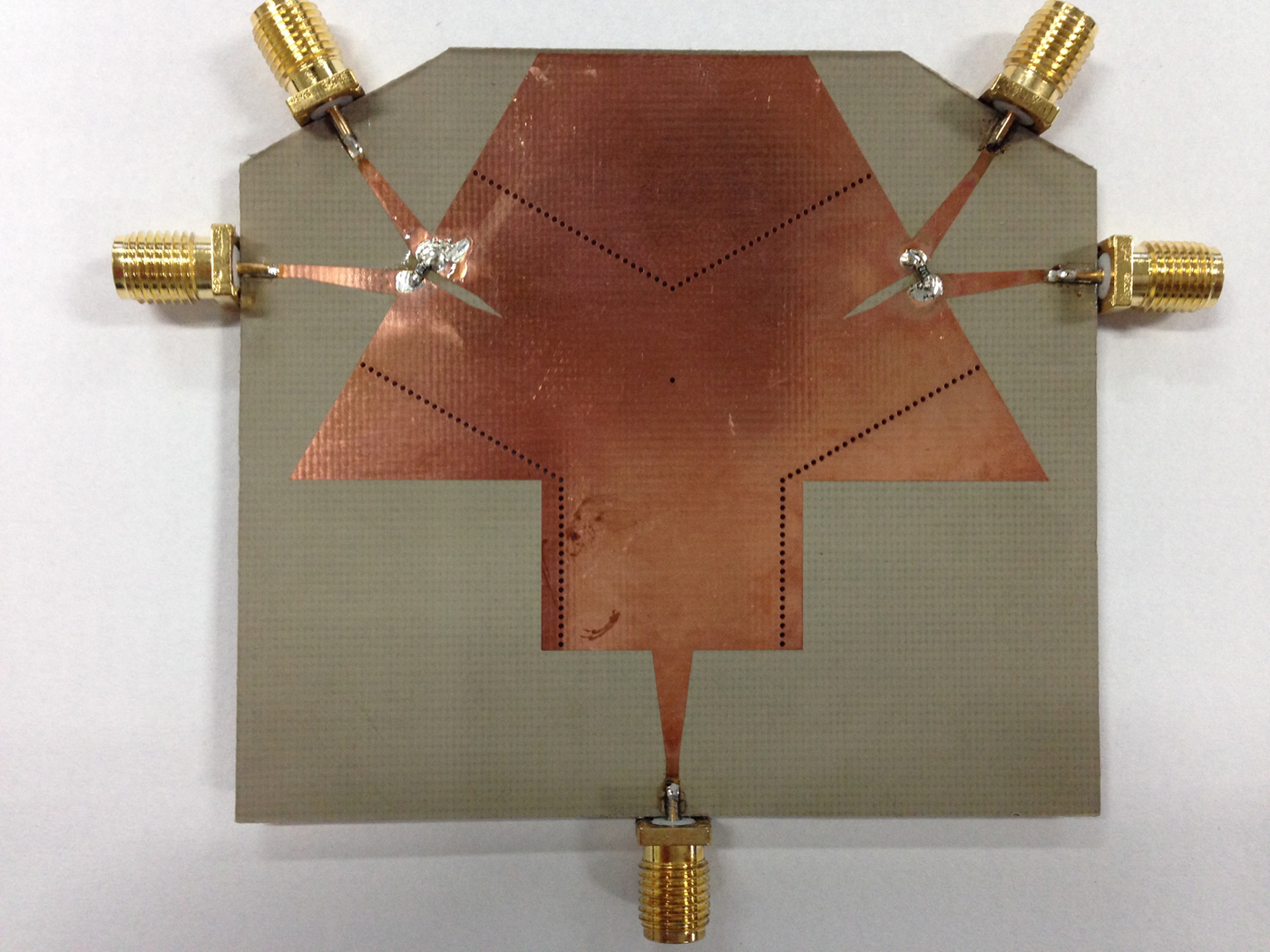
The broadband-modified four-way Y-junction PD is fabricated with a two-layer substrate Taconic RF-35 with a dielectric constant ε r of 3.5, a thickness of 0.508 mm, and a loss tangent of 0.0018. Figure 5 gives the fabricated broadband four-way Y-junction PD, and the final optimized circuit size is shown in Table 1.
Photograph of the broadband-modified four-way Y-junction power divider/combiner circuit.

Values of parameters of circuit

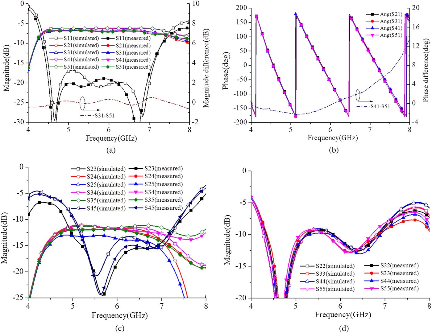
The simulated and measured results are shown in Fig. 6. It can be seen from Fig. 6(a), the center frequency of the circuit is 5.75 GHz. The simulated input return loss is larger than 15 dB, and the measured one is larger than 17 dB in a frequency range of 4.5–7 GHz. Equal power division for simulated results is achieved around 4.5–7 GHz, while the measured insertion losses are around 1.2 dB, and amplitude unbalance is about ±0.25 dB in the same frequency range. The measured results of phase relationship among output ports are shown in Fig. 6(b); it can be seen that the measured phase unbalances are ±2° from 4.5 to 7 GHz. In addition, the simulation and measured results of the isolation and the output VSWR are shown in Figs 6(c) and 6(d); it can be seen that the isolation of adjacent output ports (such as ports 2, 3 and ports 4, 5) is more than 13 dB. It is better than the non-adjacent ports isolation, which is more than 11 dB across the band 5.2–7 GHz. The better isolation is caused by isolation resistors that are loaded between the adjacent ports. As we can see from Fig. 6(d), the simulation and measured results of the output return loss are both better than 15 dB. The measured results are in good agreement with the simulated ones, and the small difference between the two is mainly caused by the manufactural error. The increase of the insertion loss is mainly caused by the conductor loss of the substrate and the loss of the SMA joint.
Simulation and test results of broadband-modified four-way Y-junction power divider/combiner circuit: (a) input return loss and insertion loss; (b) phase; (c) isolation; (d) output return loss.

Conclusion
In this paper, a broadband-modified four-way Y-junction SIW PD/combiner based on the traditional Y-junction waveguide is proposed. The broadband equal power ratio is achieved by using direct transition structure from SIW to HMSIW. The isolation and the VSWR bandwidth are improved by loading the isolation resistor between HMSIW in the output ports. The design is analyzed by the even- and odd-mode analysis method. The measured average insertion loss of the broadband-modified four-way Y-junction PD/combiner is approximately 1.2 dB and the return loss is >17 dB from 4.5 to 7 GHz. A maximum amplitude imbalance of ± 0.25 dB and a phase imbalance of ±2° are observed over the entire operating frequency range. The measured and simulated results show good agreement with each other over the operating frequency range.
Acknowledgement
This work was supported by the National Natural Science Foundation of China (Grant No: 61771094).
 Kaijun Song (M'09-SM'12) received the M.S. degree in Radio Physics and the Ph.D. degree in Electromagnetic Field and Microwave Technology from the University of Electronic Science and Technology of China (UESTC), Chengdu, China, in 2005 and 2007, respectively. In 2011, he received the “New Century Excellent Talents in University Award” from the Chinese Ministry of Education. In 2014, he received the academic and technical leaders in Sichuan province. Since 2007, he has been with the EHF Key Laboratory of Science, School of Electronic Engineering, UESTC, where he is currently a Full Professor. From 2007 to 2008, he was a postdoctoral research fellow with the Montana Tech of the University of Montana, Butte, USA, working on microwave/millimeter-wave circuits and microwave remote-sensing technology. From 2008 to 2010, he was a research fellow with the State Key Laboratory of Millimeter Waves of China, Department of Electronic Engineering, City University of Hong Kong, on microwave/millimeter-wave power-combining technology and ultra-wideband (UWB) circuits. He was a senior visiting scholar with the State Key Laboratory of Millimeter Waves of China, Department of Electronic Engineering, City University of Hong Kong in November 2012. He has published more than 150 internationally refereed journal papers. His current research fields include microwave and millimeter-wave/THz power-combining technology; UWB circuits and technologies; microwave/millimeter-wave devices, circuits, and systems; and microwave remote-sensing technologies. Prof. Song is the Reviewer of tens of international journals, including Scientific Reports, IEEE Transactions, and IEEE Letters.
 Zihang Luo was born in Chengdu, China in 1991. He received the Bachelor of Science degree in Physics from the University of Electronic Science and Technology of China (UESTC), Chengdu, China, in 2015, and now he is trying to obtain his Master degree in Electrical Engineering in UESTC. His current research interests include millimeter-wave techniques with a focus in RF/microwave passive.
 Song Guo was born in Lang Fang, Hebei Province, China, in February 1993. He received the B.Sc. degree in Microelectronics from Harbin Engineering University, Harbin, Heilongjiang, China, in 2006, and is currently working toward the M.Sc. degree in Electromagnetic Fields and Microwave Technology at the University of Electronic Science and Technology of China (UESTC), Chengdu, China. His research interests include microwave and millimeter-wave power-combining technology and microwave passive component design.
 Maoyu Fan was born in Chongqing, China, in 1991. She received the Bachelor of Science degree in Physics from the University of Electronic Science and Technology of China (UESTC), Chengdu, China, in 2014, and is currently working toward the Master degree in the School of UESTC. Her current research interests include electromagnetic, metamaterials and microwave/millimeter-wave devices, circuits, and systems.
 Yedi Zhou was born in Harbin, Heilongjiang Province, China, in January 1991. He received the B.S. degree from the University of Electronic Science and Technology of China (UESTC), Chengdu, China, in 2013. He is currently pursuing the Ph.D. degree in Electromagnetic Fields and Microwave Technology at UESTC. His research interests include microwave and millimeter-wave power-combining technology.