I. INTRODUCTION
Emerging wireless transmitter architectures have recently been receiving a lot of attention from both industry and academics. In comparison to the still more common I/Q or Cartesian transmitter, Tx, architecture, a polar topology can achieve a much better trade-off between nonlinear distortion and supply power efficiency. Derived from the envelope elimination and restoration (EER) or Kahn [Reference Kahn1] concept, a polar Tx circumvents the compromise representing the complex envelope using amplitude and phase signals, a x(t) and φ x(t), respectively, which are then treated independently until the last Tx stage, the RF PA. The power amplifiers (PA) is in fact a switching device, typically operating in a highly efficient class D−1, E, F, or F−1 mode, whose excitation signal is a constant envelope φ x(t) modulated carrier, while a x(t) is finally restored dynamically modulating the PA's supply voltage, v DD(t). In Fig. 1, a system-level model of such architecture is presented.
System model of a wireless Tx with polar architecture.

Unfortunately, as in the case of any other engineering solution, this architecture does not follow an ideal distortion-free operation, presenting a series of nonlinear impairment mechanisms at device, circuit, and system levels.
In [Reference Raab2], Raab treated the finite AM modulator bandwidth in an approximate way, assuming an ideal brick-wall reconstruction filter, while the differential delay between the AM and PM paths was studied considering this delay as fixed and independent of the base-band envelope frequency. Later, the finite bandwidth analysis was extended by Milosevic et al. in [Reference Milosevic, van der Tang and van Roermund3], where a general reconstruction filter was considered.
In [Reference Wang, Peng, Yousefzadeh, Maksimović, Pajić and Popović4], Wang et al. experimentally investigated the distortion caused by v DD(t)-to-a y(t) nonidealities, v DD(t)-to-φ y(t) conversion, and differential delay. There, they recognized that v DD(t)-to-a y(t) presented a certain degree of nonlinearity, as the tested class E PA presented carrier feedthrough, i.e., the pressed a y(t) levels off to a non-null value when v DD(t) goes to zero.
In the present paper, the impact of the main nonidealities appearing in a polar transmitter will be addressed. Special attention will be paid to the identification of the limiting factors of device operation as an RF switch, AM modulated through the supply voltage. Circuit design guidelines and implementation considerations will also be presented, with emphasis on the modulating stage and the envelope amplifier (EA). An analytical model of the nonlinear distortion in a polar transmitter will be included, together with system-level simulation results for the clasical two-tone linearity test or under real telecommunication signals. The results to be presented were obtained from the joint work of several European institutions inside the TARGET Network of Excellence. In particular, such results were derived from Task D activities inside Work Package 2.3.2 WiSELPAs.
II. IDENTIFICATION OF TRANSISTOR LIMITING FACTORS FOR HIGHLY EFFICIENT RF SWITCHING
In polar transmitters, a switched mode power amplifier, handling a phase-modulated carrier, is usually modulated in amplitude by means of the drain supply voltage. A highly efficient and linear operation along the whole modulating range is then desired for properly overcoming the limitations of I/Q transmitting architectures.
A) Switching models
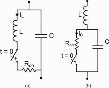
In switched mode PAs, the devices are used as high-speed switches rather than controlled current sources as in traditional power amplifiers. To first order, the devices may therefore be modeled by either of the simplified switch models shown in Fig. 2.
Idealized switch models: (a) series inductance loss model and (b) parallel capacitance loss model.

In general, most devices are best described by the model in Fig. 2(b), where the output capacitance is in parallel to the switch (i.e., the intrinsic channel region) and the series inductance is an extrinsic parasitic mainly present due to the device package. Both models also include a finite on-resistance, R on. In switched mode PAs, the switch is periodically closed and opened with the RF input signal as a stimulus. For model (b) in Fig. 2, any voltage, V c, present over the switch when it closes will result in wasted energy in the switch resistance according to

To maximize the efficiency and enable high-frequency operation, it is therefore crucial to make sure that V c is zero when the switch closes. By a careful design of the transistor load network, zero voltage switching (ZVS) can be obtained. A number of classes of switched mode power amplifiers have been derived, including classes E, D, E/F, and F.
B) Device limitations in class E PAs
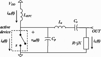
Since one of the most popular and effective switching mode PA configurations is the class E amplifier, its operation and intrinsic limitations will be focused on in the following. The basic circuit configuration of a class E PA is depicted in Fig. 3, where the active device is represented by a switch and the capacitor C p includes both device output parasitic reactance and circuit stray capacitances, and may be eventually increased by an external capacitor (if required).
Circuit schematic of a class E PA.

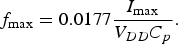
Once the capacitor value, C p, is determined from optimum circuit conditions [Reference Sokal5], the maximum operating frequency can be obtained as in (2).
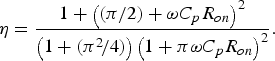
Besides, if a nonzero ON resistance for the switch is considered, R on, the stage efficiency becomes [Reference Mader, Bryerton, Markovic, Forman and Popovic6]
C) Device technology comparison
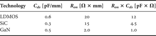
Following (3), it seems clear that to maximize the efficiency in class E PA, the R on × C p product should be minimized. Taking into account that the maximum frequency where class E operation is possible, f max, occurs when C p is completely absorbed by device parasitic output capacitance (C ds in FET families), and that the R on × C ds product is mainly determined by the device technology, different results would be expected if the PA is designed using LDMOS, SiC MESFETs, or GaN HEMTs.
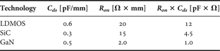
The device parameters given per millimeter gate width are summarized in Table 1. Apparently, GaN technology is shown to be superior for realization of high-performance switched mode PAs. This is also verified in recent publications, where class E and F GaN HEMT PAs having peak PAE values of 85% are demonstrated [Reference Schmelzer and Long7, Reference Pribble, Milligan and Pengelly8].
Device technology comparison for switched mode operation
III. IDENTIFICATION OF TRANSISTOR LIMITING FACTORS FOR LINEAR AM MODULATION
In analogy to the AM–AM and AM–PM conversion characteristics of linear amplifiers, the amplitude and phase nonlinearities of drain-modulated switched mode PAs are quantified through the V dd-to-AM and V dd-to-PM curves.
A) V dd/AM and V dd/PM characterization
The V dd/AM and V dd/PM profiles are usually measured using a continuous wave RF excitation at the desired input power level and sweeping the drain to source biasing voltage. Strong deviations, as carrier feedthrough or AM saturation, may be easily identified; however, the existence of mild nonlinearities may not be that evident.
To improve the accuracy of such characterization, a procedure for experimentally extracting the coefficients of their Taylor series expansions, as appearing in (4) and (5), has been developed.


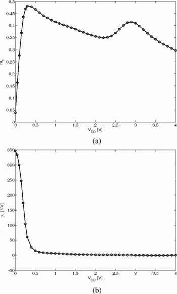
A low-level and low-frequency AM modulating tone was added to the DC voltage and inserted by the drain biasing path. The switching PA output was captured, using a vector signal analyzer, and the harmonic content of the amplitude and phase components of the complex envelope (obtained through FFT) used for extracting the m's and p's. In Fig. 4, as a way of illustration, the evolutions of m 1 and p 1 are presented for the Tx line class E PA in [Reference Pedro, García and Cabral9].
Evolution of (a) m 1 and (b) p 1 for a PHEMT-based Tx line class E PA.

Different nonlinearities are evident from the measured profiles. Besides the expected RF carrier leakage and amplitude saturation, further nonlinearity was found. At medium drain-to-source voltages, V DD around 2.5 V, the information provided by the derivatives allowed detecting a slight curvature in the V dd-to-AM characteristic, a nonlinearity associated in this case to the existence of a kink effect in the employed PHEMT device.
B) Modeling V dd/AM and V dd/PM nonlinearities
Assuming the active device switches between a state of maximum voltage (v OMAX) with minimum (ideally null) current, located in cut-off, and another one, located in the triode zone of FETs, where the current is maximum (i OMAX) and the voltage reaches its minimum (v Omin), the device current may be approximated by a semi-sinusoidal arc and the output voltage by a square wave (the case of a class F PA).
As was demonstrated in [Reference Pedro, García and Cabral10], the device fundamental output current will be the sum of a channel and a gate-to-drain current component:

This simplified model shows that, for high v DD values, i.e., when the resistive channel current dominates, the output fundamental component amplitude will be proportional to v DD, while its phase will be close to zero (or to any other constant offset). When v DD tends to zero, the capacitive current dominates over the channel current and the PA shows an evident feedthrough. There, the output amplitude tends to a constant (i.e., independent of v DD(t)), while the phase tends to −90°. Using a simple nonlinear model for C gd and a polynomial for the resistive part of a y(v DD), see [Reference Pedro, García and Cabral10] for details, a good reproduction of the V dd/AM and V dd/PM characteristics for the above-introduced Tx line class E PA was obtained, as depicted in Fig. 5.
Measured and modeled (a) v DD(t)-to-a y(t) and (b) v DD(t)-to-φ y(t) characteristics of the PHEMT-based class E PA circuit.

IV. CIRCUIT DESIGN GUIDELINES
A) Optimum operating conditions in the RF PA
For a certain gate-to-source biasing voltage, using too much input drive could exacerbate the feedthrough nonlinearity at low output levels (low values in the amplitude signal). However, using too little RF excitation could take the device out of the switched mode of operation at high values of the modulating component, resulting in increased nonlinearity at high output levels.
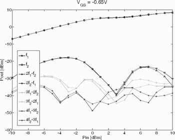
Thus, an optimum operating region could be expected, observed around 3.5 dBm for the already modeled PA – see Fig. 6. The desired tones do not vary with the RF drive and the intermodulation distortion components are minimized.
Modulating stage linearity evolution with the RF power level.

B) Design of a high-efficiency modulator
Included in the system level diagram of Fig. 1, an EA is needed to provide the supply modulating voltage. Since the total efficiency of a polar amplifier is given by PAETOT = PAEPA × η EA, it is therefore extremely critical to also maximize the EA efficiency (η EA).
As a result from the nonlinear Cartesian-to-polar transformation, the new signal components a x(t) and φ x(t) no longer have the same properties as the original I/Q data. Most importantly, the AM envelope and RF input signals are much more wideband than the original signal.
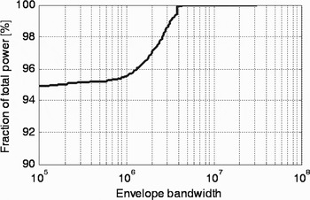
Taking a closer look at the envelope signal, it can be seen that most of its energy is concentrated at low frequencies. As a way of example, Fig. 7 shows the fractional energy content evolution versus bandwidth for the envelope of a 5 MHz WCDMA signal. Indeed, 95% of the signal energy is concentrated below a 100 kHz bandwidth.
Fractional energy content versus bandwidth for the envelope of a 5 MHz WCDMA signal.

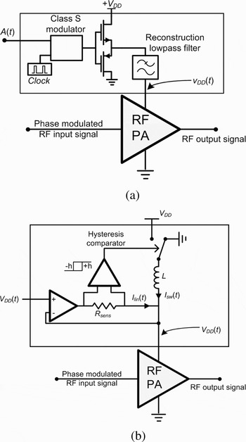
The two types of EA topologies most commonly considered in polar transmitter applications are class S modulator based, and switch mode-assisted linear amplifiers, whose simplified schematics are depicted in Fig. 8. Both have evolved from high-power/high-efficiency audio applications [Reference Kimball11, Reference Nam-Sung, Nam-In and Gyu-Hyeong12].
(a) Class S and (b) switch mode-assisted linear amplifiers.

In a class S modulator, a pulse train is generated whose low-pass filtered content corresponds to the desired signal envelope. The pulse train is amplified via a totem-pole arrangement of two transistors. The basic configuration uses complementary transistors, but since the modulator sampling clock needs to be much higher than the bandwidth of the envelope in order to maintain high signal fidelity, this tends to degrade the efficiency at wide bandwidths. This arrangement has been used for realization of EAs in low-power handset applications [Reference Jau-Horng, Fedorenko and Kenney13], but has not yet been demonstrated in high-power applications.
In the case of the switch mode-assisted linear amplifier, represented in Fig. 8(b), the topology consists of a linear stage (represented by an operational amplifier) in parallel with a switching stage.
The switching stage is controlled so as to minimize the current from the linear one. The current through the linear stage is sensed via a resistor and a hysteresis comparator. The switching block will thereby toggle state whenever the current through the linear stage exceeds the hysteresis threshold. The time constant determining the switching speed is controlled by the sense resistor, the inductance, the load resistor, and hysteresis.
The linearity of the EA is maintained by introducing a feedback from the output node to the negative input of the linear stage. The switching noise is thereby automatically canceled in the output signal, which is an important advantage compared with the class S modulator concept.
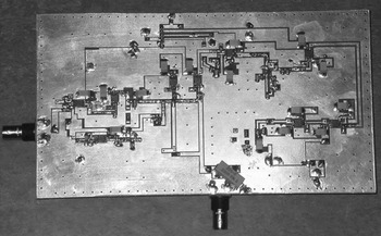
A switch mode-assisted linear EA prototype has been designed at the Chalmers University of Technology, following the topology in Fig. 8. In Fig. 9, a picture of its implementation is included.
EA PCB layout with switching, linear, and current sensing stages included.

Simulations have verified the switch mode-assisted linear amplifier concept for EAs in polar transmitters.
There are a number of design parameters to be considered and to be optimized to maximize its performance. In general, in order to significantly improve the EA efficiency beyond the 55% obtained from simulations, it is necessary to increase the switching frequency. In this way, contributions from the less efficient linear stage can be minimized. However, this requires fast switching devices and a fast feedback loop with wide bandwidth.
V. SYSTEM-LEVEL CONSIDERATIONS IN POLAR TRANSMITTERS
A) Analytical model of the nonlinear distortion
The model considered herein was developed in [Reference Pedro, García and Cabral9, Reference Pedro, García and Cabral10], based on the system level description of the transmitter shown in Fig. 1. The model includes the distortion caused by the a x(t) bandwidth limitations, differential delay, v DD(t)-to-a y(t), and v DD(t)-to-φ y(t) nonlinearities. An ideal behavior of the base-band circuitry and PM modulator was assumed. Figure 10 reports measured and simulated results of the fundamental, third-, and fifth-order IMD, obtained for varying the differential delay between paths, τ, also including the complete nonlinear model briefly discussed in section III.B. It helps us understand the relative influence of the v DD(t)-to-a y(t) and v DD(t)-to-φ y(t) nonlinearities when considering the modulating stage as part of the polar transmitting architecture.
Measured and simulated fundamental, third-, and fifth-order IMD, when τ was varied from 0 up to 5 µs [2π/(4ω m)], including both the v DD(t)-to-a y(t) and v DD(t)-to-φ y(t) nonlinearities.

As can be appreciated from Fig. 10, and according to the explanation given by the authors in [Reference Pedro, García and Cabral10], not only the distortion floor, but also the asymmetry, may be predicted when the model employed in the simulations also includes the phase nonlinearity.
Attention was then turned to the effects of the low-pass reconstruction filter, F(ω). For that, a 3 dB ripple third-order Chebyshev approximation was supposed. Figure 11 illustrates the corresponding responses predicted by the complete nonlinear model.
Measured and simulated fundamental, third-, and fifth-order IMD, when the pass-band edge frequency of the reconstruction filter was varied from Ω = ω 0/ω m = 2 up to 20, including both the v DD(t)-to-a y(t) and v DD(t)-to-φ y(t) nonlinearities.

The agreement between measured, simulated, and analytically predicted results is very good, which fully validates the model proposed in [Reference Pedro, García and Cabral10].
B) Polar transmitter simulation results under real telecommunication signals
The results presented in the above section were extended to the use of different real telecommunication signals as WCDMA, EDGE, and OFDM, all derived from ADS2005A. The main system-level nonidealities described by Raab [Reference Raab2] and previously studied for a two-tone excitation were considered:
(1) delay mismatch between amplitude and phase paths;
(2) filter in the envelope path for bandwidth limitation; and
(3) combination of both the delay and filter effects.
To quantify the results the error vector magnitude (EVM) and the adjacent channel power ratio (ACPR) figures were used. The DC/DC converter in the envelope path was modeled as a low pass filter due to the required filter for harmonic suppression.
As a way of illustration, Fig. 12 shows simulation results under WCDMA when both the filter and delay effects were included into the envelope path.
Plot of (a) ACPR and (b) EVMs versus delay and cut-off frequency for WCDMA.

The graphs show ACPR and EVM results versus delay for different filter cut-off frequencies. The ACPR graph shows that increasing the delay and decreasing the filter bandwidth increases the out-of-band distortion as predicted before. The top ACPR curve has a cut-off frequency of 0.1 MHz and therefore experiences a large amount of distortion due to the filter cut-off frequency being far less than the bandwidth of the signal (3.84 MHz).
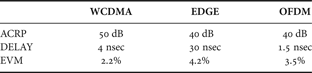
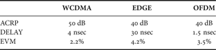
Analyzing the impact of delay and bandwidth over different communication standards, strict requirements have been obtained for achieving the desired ACPR. The results for the case of delay are summarized in Table 2.
Impact of differential delay
To fit the linearity requirements of modern standards, strict control over the architecture nonidealities is required. However, the remaining nonlinear distortion sources, associated to the modulating stage (including also the EA), demand the use of correcting or predistorting functions. Several research lines in this sense have been recently opened with the participation of the groups involved in this work [Reference Cabral, Pedro, García and Cabria14–Reference Draxler, Zhu, Yan, Kolinko, Kimball and Asbeck16].
VI. CONCLUSION
In this paper, a dedicated study of polar transmitters, as emerging and promising wireless transmitter architecture, has been presented. In theory, this technique may help overcome the current limit on achievable linearity and efficiency figures. Device, circuit, and system-level aspects have been extensively treated. Based on an accurate characterization and identification of the limiting factors of transistor operation as a RF switch, AM modulated through the supply voltage, some guidelines have been offered for selecting the optimum operating conditions of the modulating stage. Special attention has also been focused on the impact and critical design of the EA. The system-level nonidealities have been finally evaluated with both two-tone closed-form expressions and real telecommunication signal simulations.
These results were obtained as part of the work developed inside Task D of TARGET Work Package 2.3.2 WiSELPAs, a WP initially aimed to envisage future perspectives of collaboration research beyond TARGET NoE.
ACKNOWLEDGEMENT
This work was supported by the EU network TARGET “Top Amplifier Research Group in a European Team” (IST-1-507893-NOE).
 José A. Garcia was born in Havana, Cuba, on January 1966. He received a telecommunication engineering degree from the Instituto Superior Politécnico “José A. Echeverría” (ISPJAE) in 1988, and a Ph.D. degree from the University of Cantabria, Santander, Spain, in 2000.
From 1988 to 1991, he was a Radio System Engineer at a High-Frequency Communication Center, being appointed as Instructor Professor in the Telecommunication Engineering Department, ISPJAE, in 1991. From 1999 to 2001, he was an RF/Microwave Design Engineer in Thaumat Global Technology Systems and TTI Norte. He has been with the University of Cantabria since 2002, first as a Senior Research Scientist and currently as an Associate Professor. His main research interests include nonlinear characterization and modeling of active devices, intermodulation distortion control on RF and microwave applications, as well as active antennas and arrays.
 José C. Pedro was born in Espinho, Portugal, on 7 March 1962. He received diploma, doctoral, and habilitation degrees in electronics and telecommunications engineering, from the University of Aveiro, Portugal, in 1985, 1993, and 2002, respectively.
From 1985 to 1993, he was an Assistant Lecturer at University of Aveiro, and a Professor since 1993. Currently, he is a Full Professor at the same university, and a Senior Research Scientist at the Institute of Telecommunications.
His main scientific interests include active device modeling and the analysis and design of various nonlinear microwave and optoelectronics circuits; in particular, the design of highly linear multi-carrier power amplifiers and mixers. He is the leading author of Intermodulation Distortion in Microwave and Wireless Circuits (Artech House, 2003), has authored or co-authored more than 120 papers in International Journals and Symposia, and served the IEEE in the Portuguese MTT/AP/ED Joint Chapter, the MTT-11 Technical Committee, and as a reviewer and Associate Editor for the MTT Transactions and reviewer for the MTT-IMS and the EuMC.
Prof. Pedro has served his university department as the Coordinator of the Scientific Council and he is now the Department Head.
Dr. Pedro received the Marconi Young Scientist Award in 1993 and the 2000 Institution of Electrical Engineers (IEE) Measurement Prize. In 2007 he was elected Fellow of the IEEE for his contributions to the nonlinear distortion analysis of microwave devices and circuits.
 Pedro Miguel Cabral was born in Oliveira de Azeméis, Portugal, in October 1979. He received the electrical engineering and Ph.D. degrees from the University of Aveiro, Aveiro, Portugal, in 2002 and 2006, respectively.
He is currently a Post-Doctoral Researcher with the Instituto de Telecomunicações, Universidade de Aveiro, as well as an Assistant Professor.
In 2002, he received the prize for the best electrical engineering student at the University of Aveiro and in 2004 he was finalist of the Student Paper Competition presented at the IEEE International Microwave Symposium.
Since 2006, he is a reviewer for the IEEE Transactions on Microwave Theory and Techniques.
His main research interests include active device modeling, design of microwave circuits, highly efficient power amplifiers, and polar transmitters.
 Christian Fager received the M.Sc. and Ph.D. degrees in electrical engineering and microwave electronics, from Chalmers University of Technology, Sweden, in 1998 and 2003, respectively. Currently, he is working as Assistant Professor at the Microwave Electronics Laboratory where he is a project leader in the GigaHertz Centre. His research interests are in the areas of large signal transistor modeling and high-efficiency power amplifier architectures.
 Hossein Mashad Nemati was born in Tehran, Iran, in 1980. He received his B.Sc. degree in Telecommunication Engineering from Amirkabir University of Technology, Tehran, Iran, in 2004. In 2006, he received his M.Sc. degree in microwave electronics from Chalmers University of Technology, Gothenburg, Sweden. He is currently working towards a Ph.D. degree at the Microwave Electronics Laboratory, Chalmers University of Technology. His research interests are high-efficiency power amplifiers and transmitter architectures. In 2008, he received an outstanding achievement award in the student high-efficiency power amplifier design competition at the International Microwave Symposium.
 Anding Zhu received a B.E. degree in telecommunication engineering from North China Electric Power University, Baoding, China, in 1997, an M.E. degree in computer applications from Beijing University of Posts and Telecommunications, Beijing, China, in 2000, and a Ph.D. degree in electronic engineering from University College Dublin (UCD), Dublin, Ireland, in 2004.
He is currently a Lecturer with the School of Electrical, Electronic and Mechanical Engineering, UCD. His research interests include high-frequency nonlinear system modeling and device characterization techniques with particular emphasis on Volterra-series-based behavioral modeling for RF PAs. He is also interested in wireless and RF system design, digital signal processing, and nonlinear system identification algorithms.
 Paolo Colantonio was born in Roma, Italy, on 22 March 1969. He received a degree in electronic engineering from University of Roma Tor Vergata in 1994 and a Ph.D. in microelectronics and telecommunications in 2000. In 1999, he became a Research Assistant at the same university, where since 2002 he has been a Professor of Microwave Electronics. His main research activities are in the field of nonlinear microwave circuit design methodologies, nonlinear analysis techniques, and modeling of microwave active devices.