Introduction
Wireless power transfer (WPT) is the technology of delivering energy to electrical loads through electric fields, magnetic fields and electromagnetic waves [Reference Zhang, Pang, Georgiadis and Cecati1, Reference Shinohara2]. As an emerging technology, WPT has been widely applied in emerging scenarios such as solar power stations, electric vehicle charging, and drone power supply. This also necessitates rectifiers with higher power handling capabilities. The rectifier plays an important role in the whole system and is essential for the development of WPT.
Diodes and transistors are two essential rectifier devices. The former is not capable of supporting high-power wireless energy transmission [Reference He, Lin, Wu, Li and Liu3–Reference Yu, Cheng, Gu, Wang and Huang6]. The Schottky diode rectifier in reference [Reference Cheng, Du, Chen, Wu, Han and Gu7] utilizes power distribution technology to improve its power processing capability. But the maximum power is still limited to 29 dBm. The transistor-based rectifier can effectively enhance power handling capability. According to the time-reversal duality principle proposed by Hamill, RF rectifiers designed by reversing the power flow of power amplifiers will maintain high efficiency while coping with high-power capacity scenarios [Reference Hamill8]. The GaN HEMT rectifier has significantly improved the high-power handling capability. A bias voltage for the transistor is needed, but the gate itself consumes no power. However, most rectifiers based on GaN HEMT still aim for high RF-DC conversion efficiency in a narrow band, which significantly restricts their applications [Reference Hoque, Ali, Mokri, Gopal, Chahardori, Johnson and Heo9–Reference Zhang, Gu, Cheng and Xuan11]. Therefore, it is necessary to design rectifiers to achieve broadband energy conversion. In [Reference Haider, Zhang, You, He, Dong and Wang12], the necessity of a 180° phase difference is demonstrated. Hence, a broadband phase shifter is applied in the rectifier to expand the rectifier bandwidth [Reference Zhang, Gu, Cheng and Xuan13]. However, the previous works only focus on the broadband phase shift network [Reference Haider, Zhang, You, He, Dong and Wang12, Reference Zhang, Gu, Cheng and Xuan13] and the broadband rectification efficiency model has not presented. In particular, the operation mode will affect the bandwidth and efficiency. The continuous mode class-B/J power amplifier (PA) proposed by Cripps further extends the impedance region, making it more suitable for broadband design [Reference Cripps, Tasker, Clarke, Lees and Benedikt14]. The class-F/F-1PA has been applied to design rectifiers in previous works [Reference Zhang, Fusco, Cheng, Buchanan and Gu10, Reference Zhang, Gu, Cheng and Xuan13, Reference Abbasian and Johnson15]. Based on the time reversal duality principle, it is possible to expand the bandwidth of rectifiers by reversing continuous mode class-B/J PA. The continuous class-B/J operation mode in the rectifiers needs to be investigated due to a different loss mechanism compared to PAs.
This letter aims to extend the continuous mode class-B/J theory to the design of broadband rectifiers. The rectification efficiency model for a broadband rectifier has been presented for the first time. Based on the selected rectification efficiency, we establish the continuous mode class-B/J design space. In addition, the phase tuning network (PTN) is designed considering input and output matching networks. This paper further investigates the impact of port impedance variations on phase-shifting values. After accounting for package parameters, the impedance is converted from the current generator plane to the package plane. Finally, the designed rectifier exhibits high RF-DC conversion efficiency at the 10 W input power level over a wide frequency band.
Analysis of the proposed rectifier
The continuous mode class-B/J PA has a flexible design space, which tends to expand bandwidth. Based on the time-reversal duality principle, the power flow of the switching device can be reversed. The PA’s output receives the input power, and after RF-DC conversion, the DC signal is delivered from the drain terminal.
Theory of continuous class-B/J mode
The class-J operation mode applies a phase shift to the fundamental and second harmonic components in class-B operation mode, while maintaining the class-B output power and efficiency [Reference Mokhti, Lees, Cassan, Alt and Tasker16]. The continuous class-B/J mode introduces a variable factor to the class-B voltage waveform. The drain voltage and current waveforms in the continuous class-B/J mode are given by Equations (1) and (2):
 \begin{equation}{v_d} = {V_{\max }}(1 - \cos \theta )(1 - \alpha \sin \theta )\end{equation}
 \begin{equation}{i_d} = \left\{ \begin{array}{*{20}{c}}
{{I_{\max }}\cos \theta ,0 \leq \theta \leq \frac{\pi }{2}\& \frac{{3\pi }}{2} \leq \theta \leq 2\pi } \\[5pt]
{0,\frac{\pi }{2} \leq \theta \leq \frac{{3\pi }}{2}}
\end{array}\right. \end{equation}
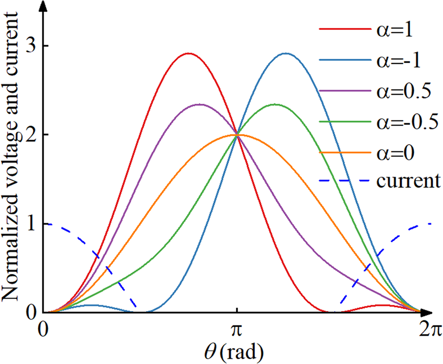
where V max represents the maximum voltage of the device and I max is the peak amplitude of the current flowing through the device. The variation of α creates a continuous design space for the fundamental and second harmonic components at the device terminals. Figure 1 shows the voltage and current waveforms of continuous class-B/J mode as α varies from −1 to 1 in 0.5 steps.
Continuous mode class-B/J current and voltage waveforms.

The expression for the fundamental and second harmonic impedance of the continuous class-B/J operation mode at the current generator plane is given by [Reference Lavandera-Hernandez, Loo-Yau, Reynoso-Hernandez, Ochoa-Armas and Moreno17]
 \begin{equation}Z_{f_0}=\frac2{\omega C_\text{out}}(1+j\alpha),\end{equation}
 \begin{equation}Z_{2f_0}=-j\frac{3\pi\alpha}{4\omega C_\text{out}},\end{equation}
where α ∈ [−1,1], C out is the nonlinear output capacitance. C out can be expressed as C out =C out0 + A[1 + tanh(B*V ds + C)], where C out0 = 1.95, A = 1192.4, B = −0.0594714, and C = −2.94696 [Reference Moon, Kim and Kim18, Reference Zhang, Cheng, Ke, Liu, Sun and Gao19].
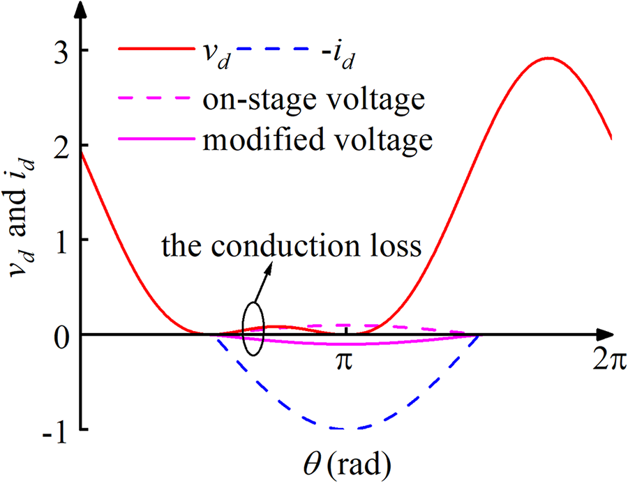
For non-ideal switches, similar to PA, the conduction loss of the rectifier is evident in the voltage waveform [Reference Abbasian and Johnson15]. The time-reversed voltage and current of the class-B/J rectifier are shown in Fig. 2. In the rectifier, the half sinusoidal pulse generated by the conduction resistance (the magenta dashed line) is modified to a negative half sinusoidal pulse (the magenta solid line) because the rectifier cannot generate negative power. The conduction loss caused by the on-state resistance Ron in continuous mode class-B/J rectifier is
 \begin{equation}{P_{{R_{{\text{on}}}}}} = \frac{1}{{2\pi }}\int {_0^{2\pi }} {R_{{\text{on}}}}{i_d}^2d\theta = {R_{{\text{on}}}}{\left( {\frac{{{I_{{\text{max}}}}}}{2}} \right)^2}\cdot\end{equation}
Current and voltage waveforms in class-B/J rectifier (α = 1).

The capacitive switching losses need to be taken into account due to the output capacitance C out in the switching devices. The output capacitance C out is charged to V max and then discharged to 0 V before the switch turns on, as determined by the drain current and voltage waveforms. Therefore, the capacitive switching loss of the rectifier can be expressed as
 \begin{equation}{P_{{\text{cap}}}} = \frac{1}{2}{C_{{\text{out}}}}V_{\max }^2\frac{\omega }{{2\pi }}\cdot\end{equation}
The dc terms in the Fourier series of the drain voltage v d and current i d mentioned in (1) and (2) can be obtained as
 \begin{equation}{V_{{\text{dc}}}} = {V_{\max }} - {R_{{\text{on}}}}\frac{{{I_{\max }}}}{\pi },\end{equation}
 \begin{equation}{i_{{\text{dc}}}} = \frac{{{I_{\max }}}}{\pi }\cdot\end{equation}
Furthermore, the dc output power of the rectifier is
 \begin{equation}{P_{{\text{dc}}}} = ({V_{\max }} - {R_{{\text{on}}}}\frac{{{I_{\max }}}}{\pi })\frac{{{I_{\max }}}}{\pi },\end{equation}
Compared to the power loss mechanism of PA, rectifiers have no overlapping losses [Reference Abbasian and Johnson15]. Therefore, in the rectifier, the total power is the sum of the power delivered to the load and the power consumed. The rectification efficiency should be
 \begin{align}\eta &= \frac{{{P_{{\text{dc}}}}}}{{{P_{{\text{dc}}}} + {P_{{\text{on}}}} + {P_{{\text{cap}}}}}} \nonumber\\
&= \frac{1}{{1 + \frac{{{R_{{\text{on}}}}{{\left( {\frac{{{I_{{\text{max}}}}}}{2}} \right)}^2}}}{{({V_{\max }} - {R_{{\text{on}}}}\frac{{{I_{\max }}}}{\pi })\frac{{{I_{\max }}}}{\pi }}} + \frac{{\frac{1}{2}{C_{{\text{out}}}}V_{\max }^2\frac{\omega }{{2\pi }}}}{{({V_{\max }} - {R_{{\text{on}}}}\frac{{{I_{\max }}}}{\pi })\frac{{{I_{\max }}}}{\pi }}}}},\end{align}
C out is negatively correlated with V ds [Reference Zhang, Cheng, Ke, Liu, Sun and Gao19]. The capacitive switching loss of the device increases with the increase of C out. A larger R on will reduce the rectification efficiency. In this paper, we assume the transistor operates in the saturation region with a drain voltage of 28 V and drain current of 1.5A.
Analysis of phase tuning network
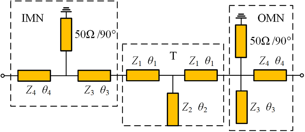
For the self-synchronous rectifier, the gate of the transistor requires an RF input signal from the drain with a 180° phase difference. An external phase shifter will degrade the rectification efficiency due to impedance mismatch at the connection. Therefore, a broadband phase shift network should be designed for the rectifier. Figure 3 shows the PTN of the rectifier, which consists of the input matching network (IMN) and output matching network (OMN) of the PA.
Phase tuning network.

As shown in Fig. 3, the ABCD parameters of the T-type structure IMN and OMN can be expressed as
 \begin{align}
&{\left[ {\begin{array}{*{20}{c}}
A&B \\
C&D
\end{array}} \right]_{\text{T}}} \nonumber \\
& = \left[ {\begin{array}{*{20}{c}}
{\cos 2{\theta _1} + \frac{{{Z_1}}}{{2{Z_2}}}\sin 2{\theta _1}\tan {\theta _2}}&{j{Z_1}\sin 2{\theta _1} + \frac{{j{Z_1}^{\text{2}}{\text{si}}{{\text{n}}^{\text{2}}}{\theta _1}\tan {\theta _2}}}{{{Z_2}}}} \\
{\frac{{j\sin 2{\theta _1}}}{{{Z_1}}} - \frac{{j{{\cos }^2}{\theta _1}\tan {\theta _2}}}{{{Z_2}}}}&{\cos 2{\theta _1} + \frac{{{Z_1}}}{{2{Z_2}}}\sin 2{\theta _1}\tan {\theta _2}}
\end{array}} \right]
\end{align}
 \begin{align}
&{\left[ {\begin{array}{*{20}{c}}
A&B \\
C&D
\end{array}} \right]_{{\text{IMN}}}} = \cos {\theta _3}\cos {\theta _4}* \nonumber\\
&\quad \left[ {\begin{array}{*{20}{c}}
{1 - \frac{{{Z_4}\tan {\theta _3}\tan {\theta _4}}}{{{Z_3}}}}&{j{Z_3}\tan {\theta _3} + j{Z_3}\tan {\theta _4}} \\
{\frac{{j\tan {\theta _4}}}{{{Z_4}}} + \frac{{j\tan {\theta _3}}}{{{Z_3}}}}&{1 - \frac{{{Z_3}\tan {\theta _3}\tan {\theta _4}}}{{{Z_4}}}}
\end{array}} \right]
\end{align}
 \begin{align}
&{\left[ {\begin{array}{*{20}{c}}
A&B \\
C&D
\end{array}} \right]_{{\text{OMN}}}} \nonumber \\
&\quad = \left[ {\begin{array}{*{20}{c}}
{\cos {\theta _4}}&{j{Z_4}\sin {\theta _4}} \\
{\frac{{ - j{Z_3}\cos {\theta _4}}}{{\tan {\theta _3}}} + \frac{{j\sin {\theta _4}}}{{{Z_4}}}}&{\cos {\theta _4} + \frac{{{Z_3}{Z_4}\sin {\theta _4}}}{{\tan {\theta _3}}}}
\end{array}} \right]
\end{align}
Further, the phase of PTN is a summation of the input, T-type and output networks. The ABCD parameters of the PTN can be inferred as [Reference Zheng, Chan and Man20, Reference Qiu and Zhu21]
 \begin{align}
&\begin{array}{*{20}{c}}
{{{\left[ {\begin{array}{*{20}{c}}
A&B \\
C&D
\end{array}} \right]}_{{\text{PTN}}}}}
\end{array} \nonumber\\
&= {\left[ {\begin{array}{*{20}{c}}
A&B \\
C&D
\end{array}} \right]_{{\text{IMN}}}}{\left[ {\begin{array}{*{20}{c}}
A&B \\
C&D
\end{array}} \right]_{\text{T}}}{\left[ {\begin{array}{*{20}{c}}
A&B \\
C&D
\end{array}} \right]_{{\text{OMN}}}}\cdot\end{align}
For the phase response, the formula of insertion phase for the PTN can be derived as
 \begin{equation}\phi_\text{PTN}=-\arctan{\left(\frac{B+CZ_0^2}{j\left(A+D\right)Z_0}\right)}_\text{PTN}.\end{equation}
The 180° phase difference between the drain and gate of the transistor needs to be satisfied in the operating frequency band, which can be expressed as
 \begin{equation}\Delta\phi=\phi_\text{IMN}+\phi_\text{T}+\phi_\text{OMN}-\theta_\text{m}=\pi,\end{equation}
where θ m is the electrical length of 50 Ω reference line. In order to ensure a constant phase over a wide frequency band, the phase slope should satisfy
 \begin{equation}\frac{d\phi_\text{IMN}}{df}+\frac{d\phi_\text{T}}{df}+\frac{d\phi_\text{OMN}}{df}-\frac{\theta_\text{m}}{f_0}=0.\end{equation}
The 2.4–3.3 GHz band is strategically significant for wireless systems, such as such as Wi-Fi and wireless power supply for civilian radar. In the following, the 2.4–3.3 GHz broadband rectifier is selected as an example to validate the effectiveness of this efficiency model. This design employs the CGH40010F transistor. The electrical equivalent circuit of the transistor is illustrated in Fig. 4(a). From the efficiency model as established in Equation (10), the output capacitance and on-resistance can be inferred. Figure 4(b) shows the relationship between the rectifier efficiency and the transistor parameters at 2.85 GHz. For η > 70%, C out varies between 1.18 pF and 2.05 pF, while R on ranges from 0.5 Ω to 2.5 Ω. Then, using (3) and (4), the desired load impedance can be obtained based on these C out. Figure 5(a) shows the corresponding design space (grey area) at the current generator plane.
The external package parameters of the transistor and the rectification efficiency model. (a) Equivalent output circuit of CGH40010F. (b) Rectification efficiency at 2.85 GHz versus C out and R on.

Design space of continuous mode class-B/J rectifier with η > 70%. (a) At the current generator plane. (b) At the package plane.

It can be seen that the impedance of the package plane can be obtained by connecting the current generator plane impedance in parallel with the equivalent circuit of the transistor. The calculation formula is as follows:
 \begin{equation}{Z_L}_{@nf_0}=\frac{(R_{22}+{Z_n}_{C_{22}})\ast Z_{n-b}}{(R_{22}+{Z_n}_{C_{22}})-Z_{n-b}}-Z_{nL_2,}\end{equation}
where:
 \begin{equation}{Z_{n - b}} = \frac{{{Z_n}_{{C_{pd}}}{Z_n}_{ - a}}}{{{Z_n}_{{C_{pd}}} - {Z_n}_{ - a}}} - {Z_{nLd}}\end{equation}
 \begin{equation}{Z_{n - a}} = \frac{{{Z_n}_{{C_{ds}}}{Z_n}_{f0}}}{{{Z_n}_{{C_{ds}}} - {Z_n}_{f0}}} - ({R_s} + {R_d} + {Z_{nLs}})\end{equation}
 \begin{equation}{Z_n}_{{C_{22}}} = \frac{{ - j}}{{n\omega {C_{22}}}},{Z_n}_{{C_{pd}}} = \frac{{ - j}}{{n\omega {C_{pd}}}},{Z_n}_{{C_{ds}}} = \frac{{ - j}}{{n\omega {C_{ds}}}}\end{equation}
 \begin{equation}{Z_n}_{{L_2}} = jn\omega {L_s},{Z_n}_{{L_d}} = jn\omega {L_d},{Z_n}_{{L_s}} = jn\omega {L_s}\end{equation}
After accounting for the package parameters of the CGH40010F, the package plane design space corresponds to the grey area in Fig. 5(b). For bandwidth extension, the drain terminal impedance needs to be designed within the aforementioned space.
Based on Equations (14) and (15), the relationship between parameters and predetermined phase shift values in the PTN can be illustrated in Fig. 6. The microstrip line impedance can be determined as 30 ≤ Z 1 ≤ 50 Ω, 40 ≤ Z 2 ≤ 70 Ω, 18 ≤ Z 3 ≤ 30 Ω and 20 ≤ Z 4 ≤ 50 Ω. The electrical length of the microstrip line can be determined as 95 ≤ θ 1 ≤ 115°, 95 ≤ θ 2 ≤ 102°, 70 ≤ θ 3 ≤ 83° and 10 ≤ θ 4 ≤ 50°. In addition, it can be observed that the phase value is less affected by θ 1 and θ 4.
Relationship between phase value and design parameters. (a) Z 1 and Z 2. (b) Z 3 and Z 4. (c) θ 1 and θ 2. (d) θ 3 and θ 4.

Measured rectification efficiency at 2.9 GHz versus (a) different V gs and (b) different R DC.

The terminal impedance of the OMN needs to be designed within the fundamental and second harmonic regions mentioned in Fig. 5(b). The OMN is analyzed based on the transmission line impedance formula. Figure 7 shows the terminal impedance and corresponding parameters in the OMN. There is an overlapping region with the impedance requirements in the PTN, ensuring both output matching and phase shift are achieved simultaneously. Z 3 and Z 4 are required to be within the range of 20–70 Ω at the fundamental frequency region of continuous class-B/J operation mode. In addition, this design takes full account of the OMN terminal impedance in Fig. 5(b).
The terminal impedance of the OMN. (a) Real part. (b) Imaginary part.

Design of the rectifier
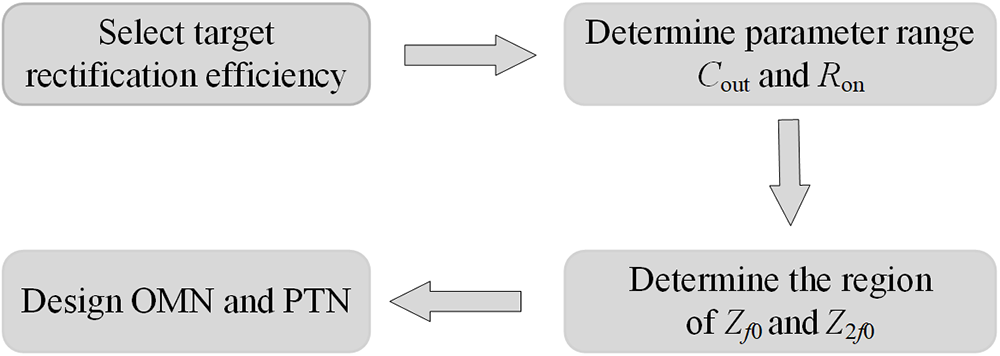
To validate the design methodology, the rectifier operating at 2.4–3.3 GHz is designed with CGH40010F. It is implemented on the Rogers 4350B with a thickness of 0.762 mm. The design flow is shown in Fig. 8. A source-pull simulation was performed to obtain the input impedance for designing the IMN. Based on the required efficiency, the output capacitance C out and conduction resistance R on were selected from Fig. 4(b). Furthermore, the fundamental and second harmonic design spaces are obtained from Fig. 5 to design the OMN. In the actual PCB design, we need to account for the welding and layout of components such as capacitors and transistor. To address these practical requirements, we made appropriate modifications, including adding solder pads and adjusting the positions of certain components. In this design, the phase of PTN is the sum of the IMN, phase shift network and OMN. It is worth noting that the PTN port impedance varies with frequency. The PTN should be adjusted to achieve 180° phase shift values over a wide frequency band. According to the above requirements, the final simulation parameters of the rectifier were optimized. The final design schematic diagram is given in Fig. 9 with a size of 3.5 × 4.4 cm2.
The design flow diagram.

The designed rectifier. (a) Schematic diagram of rectifier. (b) fabricated rectifier.

The simulated drain voltage and current waveforms at 2.6 and 2.9 GHz at the current generator plane are shown in Fig. 10. The simulated impedance traces at the package plane are plotted in Fig. 11, with the fundamental (the red line) and second harmonic (the blue line) impedance located near the theoretical continuous mode class-B/J regions. These results confirm that the designed rectifier is consistent with the continuous-mode class-B/J theory.
Drain voltage and current waveforms. (a) 2.6 GHz. (b) 2.9 GHz.

The impedance trajectory at the transistor package plane.

For the GaN rectifier, only the transistor gate needs to be supplied with initial DC bias and the gate has no power consumption. In Fig. 12(a), the designed PTN can provide a phase shift of 176°–183°. At 2.4–3.3 GHz, when the input power is 10 W, the measured saturation rectification efficiency is 66%–78%. The optimum gate voltage and load impedance at different frequency points need to be slightly adjusted. Figure 12(b) illustrates the rectification efficiency at different input powers with R DC = 50 Ω and V gs = −3.6 V.
Performance of the designed rectifier. (a) Simulated phase shift of PTN and maximum rectification efficiency with 10 W input power. (b) Measured efficiency.

The relationship between rectifier performance at 2.9 GHz and various V gs and R DC values is shown in Fig. 13. It can be seen that when V gs = −3 V and R DC = 55 Ω, the optimal rectification efficiency at 2.9 GHz can be obtained as the input power increases.
Table 1 presents the comparison results between the proposed broadband rectifier and other designs. Unlike Schottky diode-based rectifiers, the GaN HEMT transistor rectifier demonstrates greater input power capacity. In this article, the transistor operating mode is associated with the efficiency model of the rectifier, and the output capacitance and on resistance are divided and guided by the target rectification efficiency for design. Although its maximum saturation efficiency is slightly lower than some previously reported designs, it offers a broader impedance matching range. The proposed rectifier attains a frequency and power-weighted bandwidth (CFPB) that is either superior to or comparable to previously reported works. More importantly, the continuous-mode class-B/J efficiency model has been developed for this rectifier, providing a novel approach to broadband rectifier design.
Comparison with other rectifiers

Notes: C-B/J = continuous mode class-B/J; CFBP = center frequency*Pin *bandwidth; S. d = Schottky diode; G. H = GaN HEMT.
Conclusion
In this letter, a continuous mode class-B/J efficiency model for broadband self-synchronous rectifier is presented. The rectification efficiency is analyzed as a function of the capacitance C out and the on-state resistance R on. Based on the rectification efficiency model, the continuous mode class-B/J design space at the package plane is derived. The PTN is designed to conform to this impedance space. The designed broadband rectifier achieves 66%–78% rectification efficiency at an input power of 10 W with a competitive operating bandwidth. Finally, the effectiveness of the continuous class-B/J operation mode in broadband rectifiers is demonstrated.
Competing interests
The authors declare none.

Yuezhi Wu is pursuing the M.S. degree at Hangzhou Dianzi University, in Hangzhou, China. His current research focuses on phase shifters and RF power circuits.

Guohua Liu received the M.S. degree from East China Normal University, Shanghai, China, in 2004, and the Ph.D. degree in electronic science and technology from Hangzhou Dianzi University, Hangzhou, China, in 2020. He is currently a Professor with the School of Electronics and Information, HDU. His current research interests include microwave and RF circuits, sensors, antennas, and wireless communication systems design.