I. INTRODUCTION
Enhancement of GaN-based devices grown on silicon frequency performance is of increasing interest since this would enable cost-effective integration of this outstanding technology with very mature CMOS Si-based devices paving the way for novel circuit architecture with higher functionalities [Reference Chyurlia1]. For this purpose, an aggressive scaling of gate length is required while maintaining a high aspect ratio by reducing the gate to channel distance as well as the use of a short gate–drain distance in order to create a high electric field as needed for high frequency performance [Reference Awano, Kosugi, Kosemura, Mimura and Abe2, Reference Jessen3]. An attractive solution to reduce the gate to channel distance has been proposed lately [Reference Kuzmik4–Reference Medjdoub6], which consists of the use of an Al-rich ultrathin barrier layer (<10 nm) delivering extremely high two-dimensional electron gas (2DEG) carrier density. This allows avoiding the well-known gate recess technique that is difficult to control for GaN devices and may induce reliability issues at a very high frequency. However, the combination of ultrathin barrier layer and high 2DEG density induces generally a large gate leakage current that has been observed by several groups [Reference Sun7]. Recently, this limitation has been overcome for AlN/GaN high-electron-mobility transistors (HEMTs) owing to a high AlN film quality associated to a controlled surface by using an in-situ grown SiN cap layer [Reference Medjdoub, Zegaoui, Rolland and Rolland8].
Nevertheless, even though the gate leakage current has been minimized in the AlN/GaN-on-Si devices, a high 2DEG density in highly scaled GaN HEMTs may generate poor electron confinement under high bias (e.g., high electric field). A Double-heterostructure field effect transistor (DHFET) using an AlGaN back barrier is an interesting approach to enhance electron confinement [Reference Bahat-Treidel, Hilt, Brunner, Würfl and Tränkle9, Reference Micovic10].
In this work, dc, radio frequency (RF), pulsed, load-pull, and noise measurements up to 40 GHz of short channel AlN/GaN HEMTs and AlN/GaN/AlGaN DHFETs grown on silicon are presented. The benefits of the back barrier resulted in the first demonstration of high RF output power density at 40 GHz and a record f max close to 200 GHz for a GaN-on-Si device limited by the self-heating effect at drain bias higher than 15 V as seen from thermal assessment performed with an infrared camera.
II. DEVICE DESCRIPTION
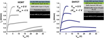
The AlN/GaN heterostructures were grown by metal organic chemical vapor deposition (MOCVD) on a highly resistive 4 inch Si (111) substrate. The HEMT structure consists of transition layers to GaN, a 1.5-μm-thick GaN buffer layer followed by a 6.0 nm ultrathin AlN barrier layer, and a 3.0-nm-thick in-situ Si3N4 cap layer (see Fig. 1). In the second structure called DHFET, the 1.5-μm-thick GaN buffer layer has been replaced with a 1.5-μm-thick Al0.08Ga0.92N layer and a 150 nm GaN channel. Room-temperature Hall measurements showed high electron sheet concentrations of 2.2 × 10¹³ and 2 × 1013 cm−2 with mobilities of 1200 and 1400 cm2 V−1 s−1 in the HEMT and DHFET heterostructures, respectively.
DC output characteristics and cross sections of a 2 × 25 µm AlN/GaN-on-Si HEMT (left) and DHFET (right) with L g = 0.2 µm. V GS swept from pinch-off to 0 V in 1 V steps.

Ohmic contacts have been formed with a Ti/Al/Ni/Au metal stack rapidly thermally annealed at 850°C directly on top of the AlN barrier layer by etching the in-situ Si3N4 layer. Device isolation was achieved by nitrogen implantation. Ohmic contact resistance (R c) extracted from linear transmission line model structures was as low as 0.35 Ωmm for both heterostructures. Then, 50 nm Si3N4 was deposited by plasma-enhanced CVD, and gate lengths (L g) ranging from 0.2 to 0.08 µm were defined by e-beam lithography. The SiN underneath the gate was fully removed by SF6 plasma etching. Another e-beam lithography step has been used in order to deposit Ni/Au gate metals. The gate–source and gate–drain spacings were 0.3 and 1 µm, respectively, and the device width was 50 µm. Finally, 100 nm Si3N4 was deposited as final passivation.
III. RESULTS AND DISCUSSIONS
A) Dc performance
Dc output characteristics of 2 × 25 µm AlN/GaN-on-Si HEMT and DHFET are shown in Fig. 1. The current density at open channel (around 1.25 A/mm at V GS = 0 V) and the maximum transconductance (470 mS/mm) are comparable for both heterostructures. However, a significant punch-through effect is observed for the HEMT structure resulting in a strong shift of the threshold voltage when increasing the drain bias. This is due to electron injection into the GaN buffer layer that is subjected to extremely high electric field in these highly scaled devices. This undesirable effect does not appear in the DHFET owing to the AlGaN back barrier that prevents parasitic electron conduction into the buffer layer, which results in a sharp pinch-off and a high breakdown voltage.
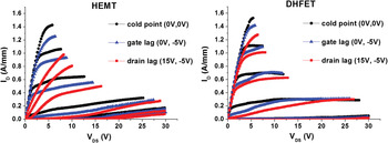
Pulsed IV for different quiescent bias points highlighting the so-called gate and drain lag effects of 2 × 25 µm AlN/GaN-on-Si HEMT and DHFET are shown in Fig. 2. Reasonably low gate lag effect is observed in both cases indicating a high material and processing quality. However, a significant drain lag effect appears for the HEMT structure due to parasitic conduction under high bias. In the case of the DHFET the drain lag effect at 15 V remains fairly low owing to substantial improvement of electron confinement.
Pulsed IV for different quiescent bias points highlighting the gate and drain lag effects of a 2 × 25 µm AlN/GaN-on-Si HEMT (left) and DHFET (right). V GS swept from pinch-off to 0 V in 1 V steps.

B) RF performance
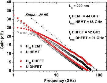
Current gain extrinsic cut-off frequencies and maximum oscillation frequencies f T = 44 and 52 GHz and f max = 68 and 91 GHz for HEMT and DHFET have been extrapolated from current gain H21 and unilateral power gain (U) at V GS = −1.6 V and V DS = 6 V, respectively (Fig. 3). The reduction of short-channel effect in the DHFET results in a slightly better f T and a decrease of output conductance that allows significant improvement of f max.
RF performance of a 0.2 × 50 µm2 AlN/GaN HEMT and DHFET on highly resistive silicon substrate at V DS = 6 V and V GS = −1.6 V.

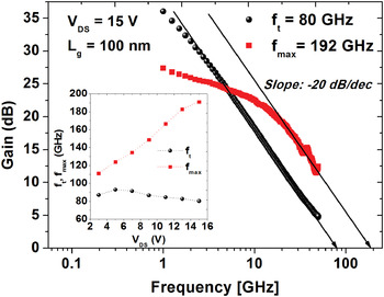
The RF performances of a sub-100 nm gate length 0.08 × 50 µm2 AlN/GaN DHFET on 4-inch Si have also been assessed (shown in Fig. 4). f T = 80 GHz and f max = 192 GHz have been measured at V gs = −1.5 V and V DS = 15 V. In spite of fairly high residual doping at the buffer/Si substrate interface resulting in RF losses of 1.5 dB/mm at 50 GHz extracted with coplanar waveguide transmission lines, excellent frequency performance has been achieved with the highest f max of GaN-on-Si transistors (as illustrated in Fig. 4). This shows the high potential of this material system for mmW applications.
RF performance of a 0.08 × 50 µm2 AlN/GaN DHFET on 4-inch Si at V DS = 15 V.

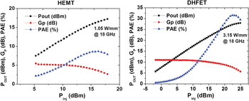
An active loadpull large-signal network analyzers (LSNA) up to 50 GHz [Reference Ducatteau, Werquin, Grimbert, Morvan and Theron11] was used to measure RF power performances up to 40 GHz. Figure 5 depicts the on-wafer continuous-wave (CW) power sweep at 18 GHz performed on a 0.2 × 200 µm2 AlN/GaN-on-Si HEMT and DHFET. At V DS = 15 V, an output power density P OUT of 1.05 W/mm with a power added efficiency (PAE) below 10% has been measured for the HEMT structure, as expected from the high drain lag effect evaluated from the pulsed measurements. On the other hand, the DHFET structure allows achieving a POUT of 3.15 W/mm and the PAE peaks above 30%, which is to the best of our knowledge the highest GaN-on-Si power density at 18 GHz with a drain bias as low as 15 V. This is due to the outstanding current density combined with a proper electron confinement.
CW power sweep at 18 GHz of a 0.2 × 200 µm2 AlN/GaN-on-Si HEMT (left) and DHFET (right) at V DS = 15 V.

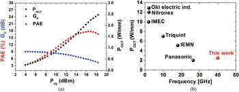
Figure 6(a) shows the CW power measurements at 40 GHz of typical 0.1 × 50 µm2 AlN/GaN-on-Si devices. An output power density of 2.5 W/mm was reached at 40 GHz when biased at 15 V which represents to our knowledge the first demonstration of high power density at 40 GHz for a GaN-on-Si transistor (as can be seen in Fig. 6(b)). The high output power results from a combination of high current density, low on-resistance, and reduced current collapse, confirmed by the dynamic load-line at V DS = 15 V acquired with the LSNA. The PAE peaks at 18% and the linear gain is about 9 dB.
(a) CW power sweep at 40 GHz of a 0.1 × 50 µm2 AlN/GaN DHFET on highly resistive silicon substrate at V DS = 15 V and V GS = −1.6 V. (b) RF power density benchmark of GaN-on-Si transistors.

The PAE is mainly limited by self-heating as well as parasitic conduction at the buffer/Si interface causing a decrease of the power gain at 40 GHz. High power operation beyond V DS = 15 V in these devices is essentially prevented by thermal effects since we noticed that current collapse and leakage current remain fairly low at higher biases. Part of our on-going work is focused on optimizing the Al content into the buffer layer in order to improve thermal dissipation in these devices and buffer/Si interface quality to enhance their large-signal gain at mm-wave frequencies. Indeed, 1.4 dB/mm losses at 40 GHz have been measured using standard coplanar waveguide lines. It has to be pointed out that the power measurements in Ka-band were performed under near-class A operation (500 mA/mm) with output matching being optimized for maximum power. No improvement in PAE was observed when the devices were biased closer to pinch-off, showing the domination of RF losses at such a high frequency.
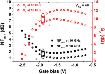
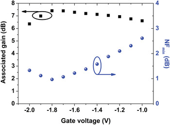
Room temperature microwave noise performance of the device has been measured at 10 and 18 GHz using the tuner method [Reference Boudiaf and Laporte12] that allows the extraction of fundamental noise parameters. Figure 7 shows the minimum-noise figure NFmin and the associated gain G A of a 0.16 × 50 µm2 AlN/GaN-on-Si transistor at V DS = 4 V. The gate leakage current was about 0.1 µA. The device exhibits an NFmin of 1 and 1.8 dB with a G A of 12 and 10 dB at 10 and 18 GHz, respectively. These data are comparable to the best reported GaN-on-Si HEMT values. It is interesting to note that the minimum noise figure corresponds systematically to the maximum G A that may allow unique monolithic integrated circuit design.
Minimum-noise figure and associated gain at 10 and 18 GHz as a function of gate bias of a 0.16 × 50 µm2 AlN/GaN-on-Si DHFET.

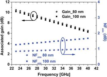
Figure 8 shows NFmin and the associated gain (G A) of a 100 nm and 80 nm AlN/GaN/AlGaN-on-Si DHFETs as a function of frequency biased at V GS = −1.8 V and V DS = 4 V. The gate leakage current was lower than 0.5 µA/mm under these conditions. G A and NFmin scale well with gate length (L g) owing to improved frequency performance with L g reduction. NFmin reaches 1 dB (1.68 dB) at 40 GHz for L g = 80 nm (L g = 100 nm) with G A remaining above 6 dB. When plotted as a function of the gate voltage, the minimum value of NFmin is 0.97 dB, with G A = 7.5 dB, at 36 GHz (see Fig. 9). As mentioned previously the optimal NFmin systematically corresponds again to the maximum G A. These datasets are the first benchmark of low noise GaN-on-Si devices in the K a band. To the best of our knowledge, this low noise performance is the best reported so far for any GaN-based transistors at such high frequency of operation. According to Fukui's Noise figure equation [Reference Fukui13], these results can be attributed to high frequency performance (f t and f max), low access and gate resistances in combination with a low gate leakage current [Reference Sanabria, Chakraborty, Xu, Rodwell, Mishra and York14] and low DC to RF dispersion observed in these devices as can be seen in Table 1 showing key device parameters of a 100 and 80 nm AlN/GaN/AlGaN-on-Si DHFET affecting noise performance.
Associated gain and minimum-noise figure as a function of frequency biased at V GS = −1.8 V and V DS = 4 V at room temperature of 100 and 80 nm AlN/GaN/AlGaN-on-Si DHFET.

Minimum-noise figure and associated gain at 36 GHz as a function of gate bias at V DS = 4 V of an 80 nm AlN/GaN/-on-Si DHFET.

Main device parameters of a 100 nm and 80 nm AlN/GaN/AlGaN-on-Si DHFET affecting noise performance according to Fukui's Noise figure equation.

C) Thermal assessment
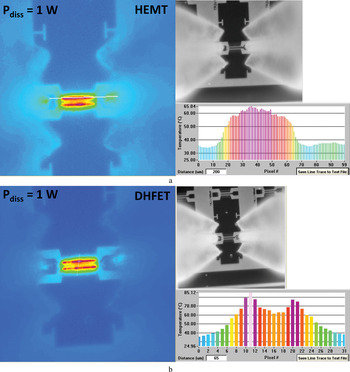
As shown in Fig. 10, an infrared camera has been used to compare the AlN/GaN-on-Si HEMT and DHFET device temperature under high bias (V DS = 25 V), corresponding to a dissipated power (P diss) of 1 W. The device temperature profiles appear in the insets where the peak is located in the gate vicinity.
Infrared camera pictures of a 2(100 µm HEMT (a) and DHFET (b) devices under bias (P diss = 1 W). The insets show device temperature profiles.

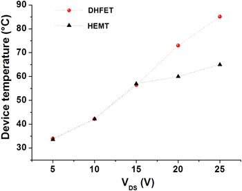
Using this set-up, the device temperature has been plotted as a function of the dissipated power for both heterostructures (Fig. 11). Similar temperatures are observed up to P diss = 0.6 W for the HEMT and the DHFET, however, at higher drain bias a significantly higher temperature is recorded for the DHFET. This results from lower thermal dissipation of AlGaN as compared to the GaN buffer layer generating a much higher thermal resistance. Therefore, the DHFET structure is mainly limited by thermal issues under high bias (V DS > 15 V) and thermal management needs to be performed in order to further enhance the GaN-on-Si RF device performance.
2 × 100 µm HEMT and DHFET device temperatures as a function of drain bias evaluated with an infrared camera.

IV. CONCLUSION
We have developed an AlN/GaN/AlGaN double heterostructure that enables aggressive downscaling of GaN-on-Si devices while delivering outstanding carrier density. DC, pulsed, small and large signal measurements as well as noise assessment confirmed the benefit of the double heterostructure for such highly scaled devices. The highest AlN/GaN/AlGaN-on-Si power density has been demonstrated at 18 GHz and V DS = 15 V as well as the first demonstration of high RF GaN-on-Si power density at 40 GHz, thermally limited at higher bias. The lowest noise performance in the K a band of any GaN-based transistor has been achieved with these devices Thus, the reduction of gate length and thermal management in the presented devices will allow unprecedented GaN-on-Si millimeter wave performances.
ACKNOWLEDGEMENT
The authors acknowledge the company EpiGaN for material delivery as well as the IEMN staff for processing support.
 Farid Medjdoub received his Ph.D. degree in Electrical Engineering from the University of Lille in 2004. He is currently a CNRS research scientist at IEMN in France. His main research interests are design and optimization of high power microwave power GaN amplifiers.
 Yoann Tagro received respectively in 2006 and 2010 the MSEE degree in Microelectronics from the University of Lille, France and the Ph.D. degree in Electrical Engineering from STMicroelectronics and the Institute of Electronic, Microelectronics and Nanotechnology (IEMN), Lille, France. His main research concerns mmW lab in-situ development, RF Noise characterization and modeling of Silicon (MOSFET & HBT) and GaN (HEMT) technologies. He holds currently a Postdoctoral position at IEMN.
 Bertrand Grimbert joined IEMN in 1984 and is currently a research engineer. His main purpose is to develop and optimize processes on III–V materials (GaAs, InP and GaN) by improving the different steps of fabrication. Since 2004, he is focused on the development of GaN devices and MMIC's for various French and European contracts and has was part of the common laboratory between IEMN and Thales (TIGER).
 Damien Ducatteau received an engineer degree from the University of Lille 1 in 1996 and the Ph.D degree in electronics at the Institut d'Electronique, de Microélectronique et de Nanotechnologie (IEMN) Laboratory, Villeneuve d'Ascq, France in 2008.
In 1997, during four years, he has been involved with the European Space Agency (ESA) within ROSETTA project, during which he has been developing the RF electronic part and the radar test procedures of the CONSERT instrument. In 2001, he joined IEMN where he has been in charge of the microwave and non linear test characterization of AlGaN/GaN HEMT devices for the common Laboratory between IEMN and THALES III–V Labs. His research activities concern the power behavior of electronic devices and he is mainly involved with the nonlinear characterization at high frequencies. Since 2006, he is the Head of the technical team that has in charge the common microwave facilities of IEMN.
 Nathalie Rolland received an Engineer degree in electrical engineering in 1986, a PhD degree in electronics from the University of LILLE in 1989 and a HDR degree in 2002. She is currently Professor at the University of LILLE at the engineer school of Polytech'lille and develops research at IEMN. She is head of the Circuit System and Microwave Application group of IEMN. From 1989 to 2000 she has investigated quasi–optical approaches and 3D interconnects for millimetre wave devices, circuits and subsystems for radar and communication application. Since 2000 she is mainly involved in the field of advanced communication systems for smart Object Communication and sensors networks in the millimetre wave range and is responsible at IEMN of two projects on these topics. She has an extensive experience in circuits and subsystems design, assembly and characterisation.